RESEARCH..........................................................................................................................................
The Dionne group is engaged in fundamental and applied research related to plasmonic and nanocrystalline metamaterials. We are an interdisciplinary team of materials scientists, physicists, chemists, and engineers who explore these materials from their nano-scale optical and quantum mechanical properties to their implementation in nanofabricated devices. Our group is actively exploring the following research areas:
Applications of plasmonic metamaterials: Transformation optics; Broadband visible-frequency negative-index materials; Metamaterial lenses and cloaks.
Plasmon-enhanced processes for photoelectrochemistry & photovoltaics: Techniques to maximize solar-spectrum utilization in photocatalysts and photovoltaics; linear and non-linear optical processes for tuned absorption, emission and lifetimes; upconversion and down-conversion in nanocrystals.
Colloidal negative index materials: Theory and assembly of visible-frequency metamaterials prepared via solution-processing.
Optical probes of bioelectromagnetism & neuronal transmission: Plasmonic and nanocrystalline materials that exhibit extreme sensitivity to local bioelectromagnetic phenomena
Quantum optical forces in nanostructures: Coupled nanocrystal-plasmon nanocavitiy systems for investigation of fundamental forces and fields.
Electrodynamics of metamaterials: Time-resolved imaging of emission into negative index media.
I. Nanoparticle Superlattice Metamaterials:
Calculations by Hadiseh Alaeian demonstrate that lattices of Au nanoparticles can exhibit emergent optical properties distinct from the constituent particles, including optical-frequency magnetism. Her results could form th basis for new, bottom-up assembled metamaterials. Her results were published in the July 2 issue of Optics Express.
II. Quantum Plasmons:
Jon Scholl and Ai Leen Koh demonstrate that metal nanoparticles with dimensions between one and ten nanometers exhibit plasmon resonances governed by quantum mechanical effects, as probed with electron microscopy and spectroscopy. Their results appear as the cover Article in the March 22 edition of Nature.
III. Nanowire Solar Metamaterials:
Recent calculations by Hadiseh Alaeian determine the ideal nanowire dimensions and lattice configuration for optimal photovoltaic conversion. Her results were published as an invited article in the Journal of Optics on January 12.
IV. Plasmonic Upconversion:
Recent calculations by Ahswin Atre indicate the potential for significant upconversion enhancements using plasmonic nanostructures. His results were published as an invited article in the Journal of Optics on January 12.
V. Plasmonic Gain:
Recent calculations by Amr Saleh indicate the potential for gain-based plasmonic devices with low required threshold gains. Properly designed plasmonic structures can strongly enhance the gain factor of nonlinear materials, despite the higher losses usually associated with metals. His results, published in Physical Review B on January 5, will enable efficient nanoscale plasmon amplifiers, spasers, and lasers.
VI. Magnetic and Electric Fano Resonances:
Recent calculations by Sassan Sheikholeslami and Aitzol Garcia demonstrate Fano-like interference effects between electric and magnetic modes in visible-frequency "metamolecules." Their results, pulished in Nano Letters on August 5, will enable exquisite spatial and temporal control of electromagnetic hotspots, with compelling applications for molecular and biosensing.
On subwavelength scales, photon-matter interactions are limited by diffraction. The diffraction limit restricts the size of optical devices and the resolution of conventional microscopes to wavelength-scale dimensions, severely hampering our ability to control and probe subwavelength-scale optical phenomena. Circumventing diffraction is now a principle focus of integrated nanophotonics. Surface plasmons provide a particularly promising approach to sub-diffraction-limited photonics. Surface plasmons are hybrid electron-photon modes confned to the interface between conductors and transparent materials. Combining the high localization of electronic waves with the propagation properties of optical waves, plasmons can achieve extremely small mode wavelengths and large local electromagnetic field intensities. For example, even x-ray wavelengths can be achieved at optical frequencies. Through their unique dispersion, surface plasmons provide access to an enormous phase space of refractive indices and propagation constants that can be readily tuned with material or geometry.
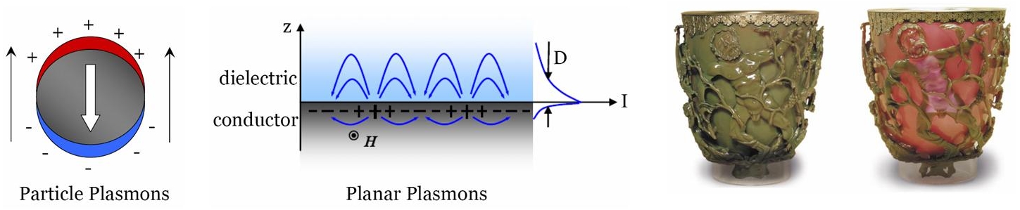
While SPs can occur at any metal-dielectric interface, particle and planar plasmon geometries have received particular attention. The figure above depicts two examples of these geometries with just one metal-dielectric interface. As seen in the schematic, particle plasmons resemble dipoles, with clouds of charge localized at the poles. At their resonant frequency, these localized surface plasmons will be characterized by a large scattering coefficient and a large extinction cross-section. Accordingly, particle-based geometries can act as optical nano-antennas, concentrating incident radiation to a subwavelength physical region. Such properties have been exploited in applications ranging from surface-enhanced Raman spectroscopy to photothermal tumor ablation. In contrast, planar plasmonic geometries are characterized by propagating charge-compression waves localized to the metal-dielectric interface. Depending on the excitation wavelength and the specific materials used, the field penetration into the dielectric can be subwavelength. Additionally, plasmon propagation lengths in planar geometries can approach centimeter scales.
Though surface plasmons have only recently been considered for optoelectronic applications, the properties of metallic nanostructures have been exploited for centuries. Both the vivid colors of stained-glass windows and the optical dishroism of the Lycergus cup, designed in the fourth-century, A.D. (shown above) derive from small metallic particles embedded in the glass. Since those early artisan studies, plasmonics has expanded to applications ranging from nanoscale optical waveguides and devices to enhanced light emission, improved photovoltaics and photocatalysts, and electromagnetic metamaterials that may enable "perfect lenses" and invisibility. The explosive growth of the field is reflected in the scientific literature: since 1990, the number of papers related to surface plasmons has doubled every five years. In conjunction with numerous US and internation groups investigating such nanoscale optical interactions, the Dionne group is hoping to make a significant contribution to the various technological challenges that will face our generation, using the power of plasmonics.
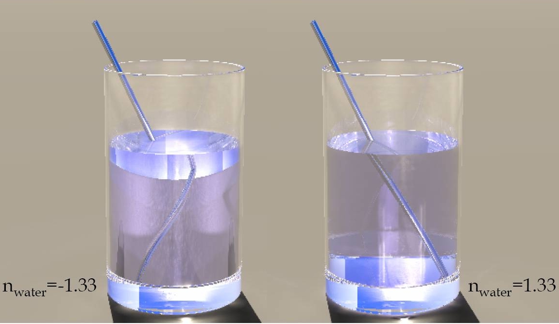
Negative index materials (NIMs) are characterized by an electric permittivity and magnetic permeability that are simultaneously negative, resulting in a negative index of refraction. Unlike naturally-occurring materials, the energy velocity of electromagnetic signals in a NIM is oriented opposite to the phase velocity. This antiparallel velocity flow gives rise to many unusual effects, including negative refraction at the interface between positive and negative index media, a reversed Doppler effect, and even negative radiation pressure (see the simulated image to the left from Dolling et al., Optics Express 2006). NIMs also serve as electromagnetic cloaks and amplify evanescent electromegnetic waves, creating the possibility for a "perfect lens" that can resolve arbitrarily-small feature sizes.
Traditional approaches to achieving a NIM involve fabricating subwavelength resonator elements to form a metamaterial. While two and three-dimensional metamaterials have been realized from microwave to near-infrared frequencies (see for example the beautiful work by X. Zhang at berkeley, V. Shalaev at Perdue, and D. Smith at Duke), scaling metamaterials down to visible frequencies has proved challenging. Achieving a NIM that operates over a broad range of visible-wavelengths remains a premier goal of the optics community, since many applications involve controlling electromagnetic radiation in the visible.
By exploiting the unique dispersion properties of surface plasmons, the first direct demonstration of all-angle negative refraction in the visible was achieved by Jen Dionne and colleagues (see the article "Negative Refraction at Visible Frequencies by Henri Lezec, Jen Dionne, and Harry Atwater in the publications section of this site). Rather than using discrete subwavelength resonators, our approach involves continuous metal-dielectric layers. For frequencies above the surface plasmon resonance but below the bulk plasma frequency, plasmons are characterized by oppositely-oriented energy and phase velocities and hence exhibit a negative refractive index. In our first experiments, negative refraction was observed across the interface between a positive index slot waveguide (similar to a fiber optic) and a negative-index metal-insulator-metal plasmonic waveguide. Negative refraction occured in the blue-green region of the spectrum, but calculations indicate that this range can be extended over the entire visible spectrum (see the article in Optics Express by Jen Dionne, Ewold Verhagen, Albert Polman, and Harry Atwater).
Current research is aimed at applying these negative index materials to optical imaging systems that overcome the Rayleigh limit, both focusing and magnifying subwavelength objects in the far-field. Research is also aimed at designing a visible-frequency electromagnetic cloak that exploits the index-tunability of modes in plasmon waveguides.
Colloidal nanocrystal are chemically-synthesized metallic or semiconducting clusters with sizes ranging from tens of nanometers down to a single nanometer. In one sense, these represent a near-ideal representation of the "particle in a box" model taught in introductory quantum mechanics. Due to their finite size, electrons and holes in these particles exhibit quantum confinement that shifts the band energies from the bulk values. Accordingly, their emission wavelengths can tuned from the ultraviolet to the infrared, simply by tuning the nanocrystal size. A variety of nanocrystal morphologies, including dots, rods, and tetrapods, can be readily synthesized, with heterojunction geometries achievable through core-shell coating and cation or annion exhange. Further, nanocrystals can be assembled into 'artifical molecules' through self-assembly or DNA-assisted assembly. Due to their vast tunability of emission and absorption wavelengths, their high degree of quantum confinement, and their low defect density, nanocrystals provide an ideal platform for subwavelength light-matter investigations. In addition, nanocrystals have been shown to exhibit a variety of unusual and exotic properties including strain-tuned photoluminescence, nonlinear processes, phonon-assisted upconversion, and multiexcitonic generation.
Facilities
The Dionne Laboratories are located in Durand Hall and will soon include a full wet-laboratory and optics laboratory. The wet-lab is designed for device fabrication and nanocrystal synthesis and includes fume hoods, gloveboxes, an evaporation and sputtering chamber, spinners, centrifuges, dual-manifold schlenk lines, and characterization equipment. The optics lab will includes optical tables equipped with far-field and confocal fluorescence microscopes, a near-field microscope, a cryogenic stage, a low-temperature electro-optic probe station, and various CW and pulsed tunable laser sources. Additional characterization and fabrication facilities, including FIB, SEM, and TEM, are located in the SNL and CIS.
Funding
Research in the Dionne group is generously supported by the Air Force Office of Scientific Research, the National Science Foundation, the Department of Energy, the Global Climate and Energy Project, a Hellman Fellowship, a Federick E. Terman Fellowship (endowed by William Hewlett and David Packard) and from a Robert N. Noyce Family Faculty Fellowship. Research support from Intel, Northrop Grumman, the Gabilan family, and Stanford University's School of Engineering is also acknowledged.