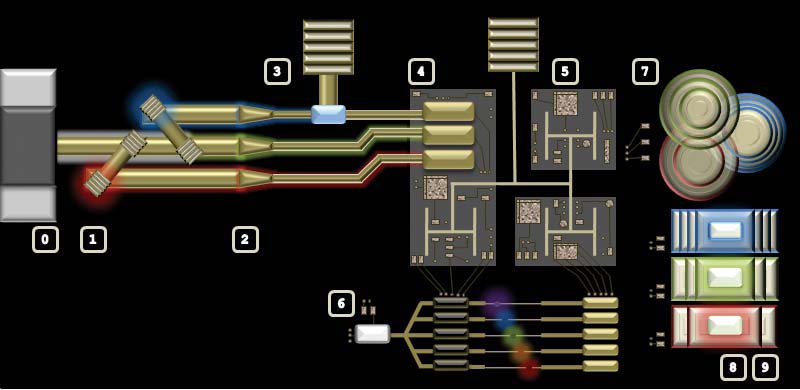
PUBLICATIONS.....................................................................................................................................


The below list highlights our recent peer-reviewed articles. Please scroll over the titles to open the abstract; access to full article content may require journal subscription. In addition to the scientific literature, our work has also been featured in popular science accounts, including Pickover's book "Archimedes to Hawking" and Kaku's book "Physics of the Impossible."
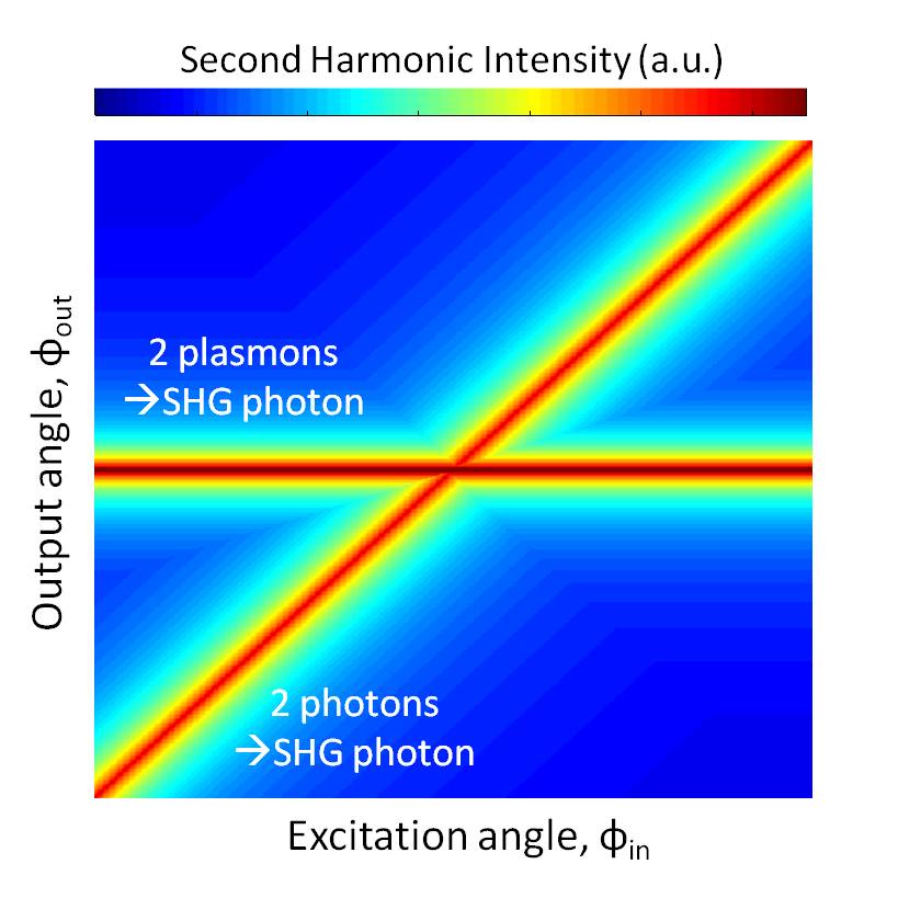
Collective electron excitations in metals, called plasmons, can play an important role in second harmonic generation of light. This Viewpoint describes results from the article "Nonlinear plasmon-photon interaction resolved by k-space spectroscopy," by Nicolai B. Grosse, Jan Heckmann, and Ulrike Woggonthe, Physical Review Letters (2012)
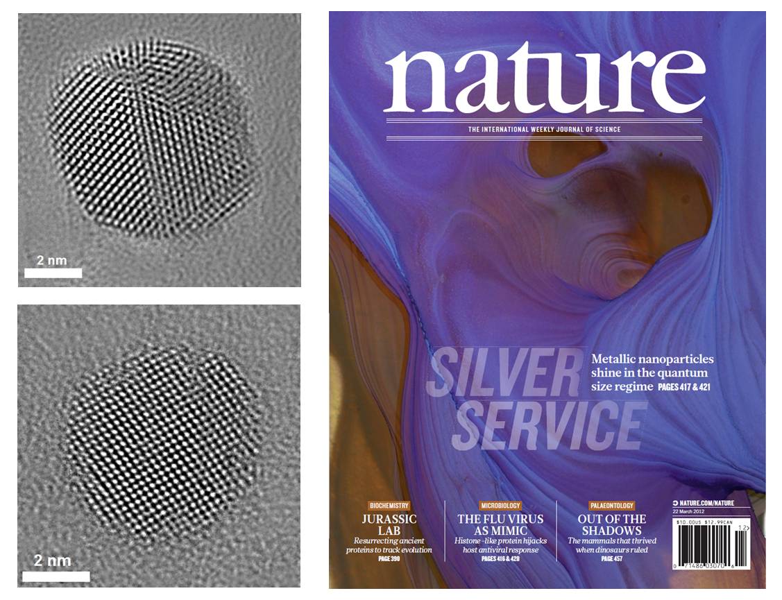
The plasmon resonances of metallic nanoparticles have received considerable attention for their applications in nanophotonics, biology, sensing, spectroscopy and solar energy harvesting. Although thoroughly characterized for spheres larger than ten nanometres in diameter, the plasmonic properties of particles in the quantum size regime have been historically difficult to describe owing to weak optical scattering, metal–ligand interactions, and inhomogeneity in ensemble measurements. Such difficulties have precluded probing and controlling the plasmonic properties of quantum-sized particles in many natural and engineered processes, notably catalysis. Here we investigate the plasmon resonances of individual ligand-free silver nanoparticles using aberration-corrected transmission electron microscope (TEM) imaging and monochromated scanning TEM electron energy-loss spectroscopy (EELS). This technique allows direct correlation between a particle’s geometry and its plasmon resonance. As the nanoparticle diameter decreases from 20 nanometres to less than two nanometres, the plasmon resonance shifts to higher energy by 0.5 electronvolts, a substantial deviation from classical predictions. We present an analytical quantum mechanical model that describes this shift due to a change in particle permittivity. Our results highlight the quantum plasmonic properties of small metallic nanospheres, with direct application to understanding and exploiting catalytically active and biologically relevant nanoparticles.
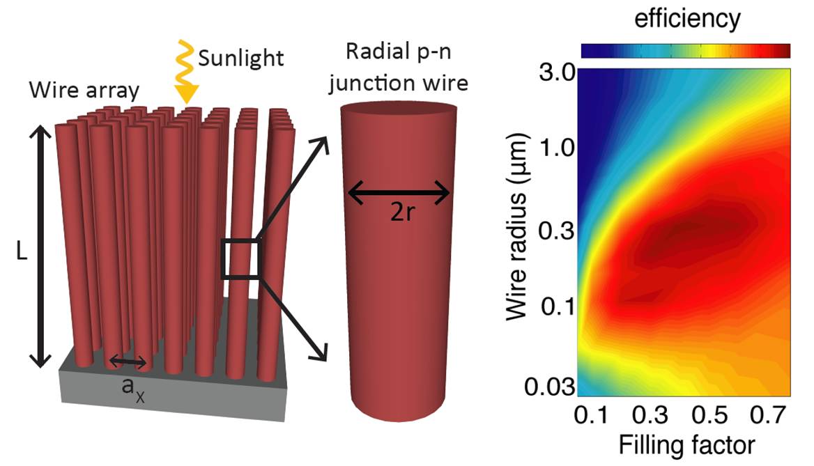
Reducing reflection and transmission losses in photovoltaic devices is essential for realizing highly efficient power conversion. Here, we theoretically investigate arrays of radial junction silicon wires to determine the optimal geometry for maximized light absorption. Using a generalized rigorous coupled wave analysis, we calculate the scattering spectra of arrays of varying wire radii, length, and lattice filling factors. Near unity absorption, far exceeding that of conventional thin film devices, is calculated for a square array of 20 µm long wires with radii of 200 nm and a filling fraction of 30%. These results suggest a potentially cost-effective route toward high efficiency solar cells.
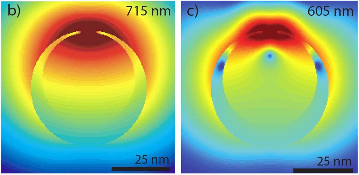
Upconversion of sub-bandgap photons can increase the maximum efficiency of a single-junction solar cell from 30% to over 44%. However, upconverting materials often have small absorption cross-sections and poor radiative recombination efficiencies that limit their utility in solar applications. Here, we show that the efficiency of upconversion can be substantially enhanced with a suitably designed plasmonic nanostructure. The structure consists of a spherical nanocrescent composed of an upconverter-doped dielectric core and a crescent-shaped metallic shell. Using numerical techniques, we calculate a greater than 10-fold absorption enhancement for a broad range of sub-bandgap wavelengths throughout the entire upconverting core. Further, this nanocrescent enables a 100-fold increase in above-bandgap power emission toward the solar cell. Our results provide a framework for achieving low-power solar upconversion, potentially enabling a single-junction solar cell with an efficiency exceeding the Shockley–Queisser limit.
Loss is one of the most substantial impediments to integrated plasmonics. In this paper, we present a theoretical analysis of active cylindrical plasmon slot waveguides, including their modal characteristics, gain spectra, and lasing threshold. Particular attention is given to two classes of waveguide geometries composed of various core/channel/cladding materials: a dielectric/dielectric/metal (DDM) waveguide and a metal/dielectric/metal (MDM) waveguide. Using empirically determined optical constants, we systematically study the dispersion, propagation length, threshold gain, modal gain, and confinement factor of these slot structures. For DDM waveguides, we show that introducing the gain in the channel rather than the core is of paramount importance for reduced threshold gain and increased modal gain. Confinement factor enhancement is even more pronounced in MDM waveguides, where modal gain can exceed threshold gain by 10× to 100× across visible and near-infrared frequencies. By carefully tuning the core/channel relative dimensions along with the lasing frequency, we show that threshold gain as low as 500 inverse cm is achievable in cylindrical plasmonic devices with overall diameters less than 200 nm. Our results indicate the promise of plasmonic slot structures for low-loss optical networking, and provide a roadmap for the design of optimized nanoscale plasmonic laser cavities.
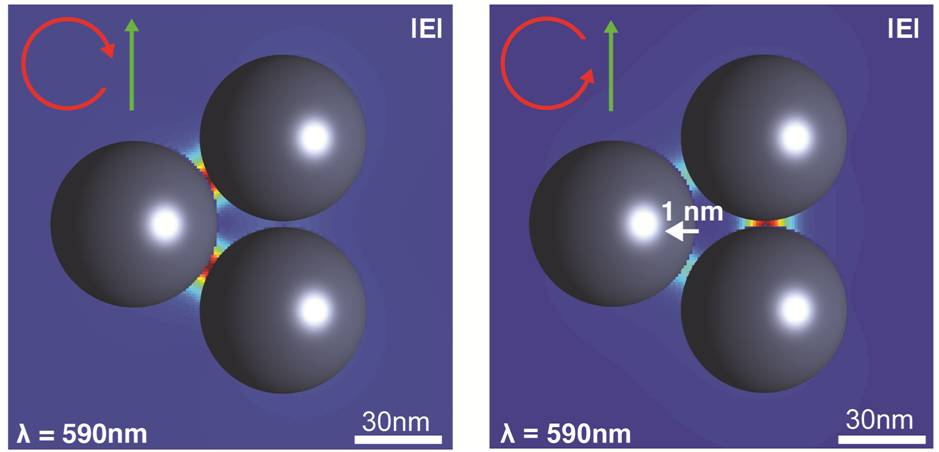
Assemblies of strongly coupled plasmonic nanoparticles can support highly tunable electric and magnetic resonances in the visible spectrum. In this letter, we theoretically demonstrate Fano-like interference effects between the fields radiated by the electric and magnetic modes of symmetric nanoparticle trimers. Breaking the symmetry of the trimer system leads to a strong interaction between the modes. The near and far field electromagnetic properties of the broken symmetry trimer are tunable across a large spectral range. We exploit this Fano-like effect to demonstrate spatial and temporal control of the localized electromagnetic hotspots in the plasmonic trimer.
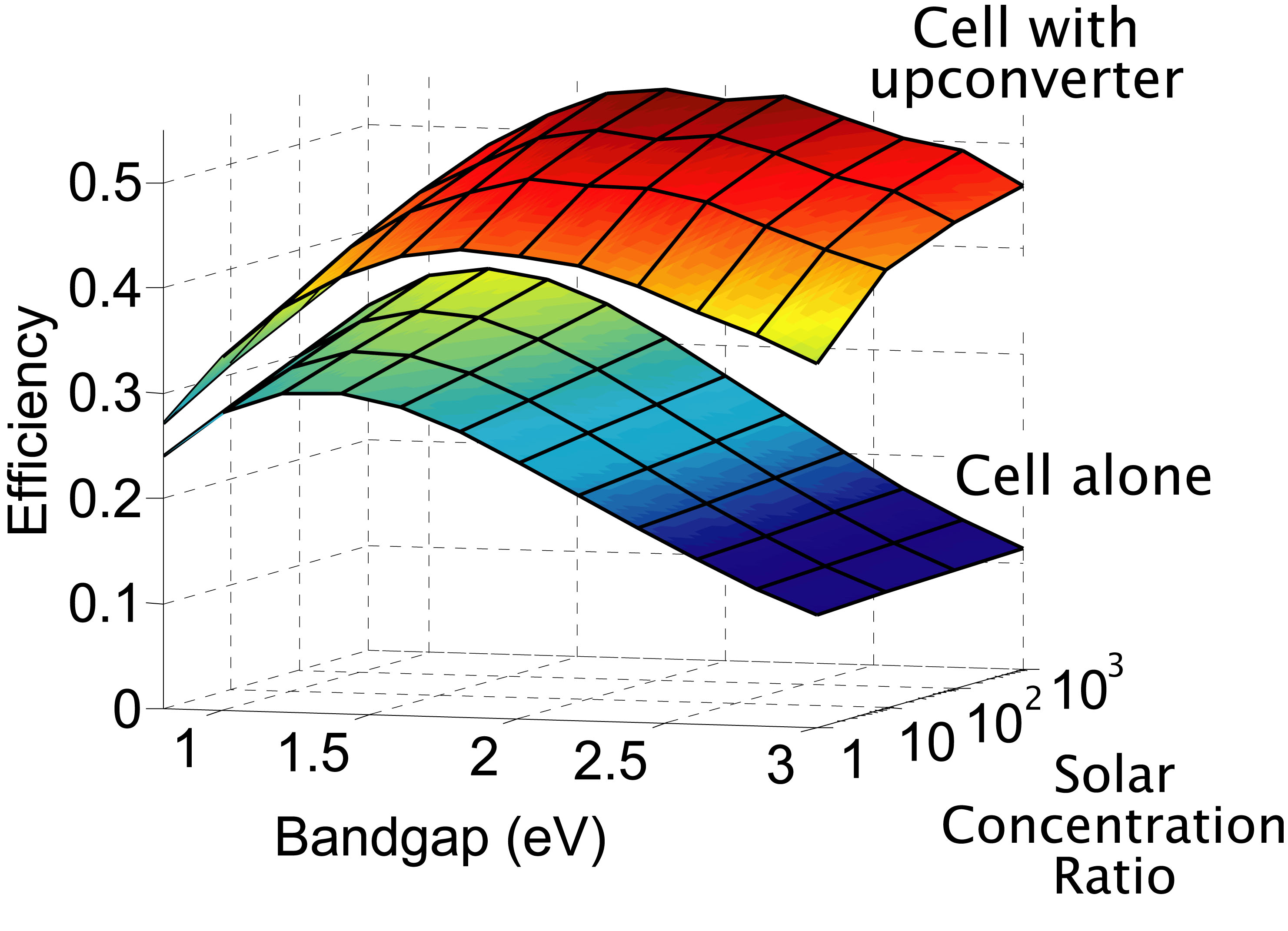
Upconverting materials can be used to increase the energy conversion efficiency of a solar cell. Such materials convert low-energy transmitted photons to higher-energy photons that can be absorbed by the cell, substantially reducing the spectral mismatch between the cell and the solar spectrum. Previously, the performance enhancements achievable with an ideal upconverter-solar cell system were theoretically investigated. Here, we perform a comprehensive analysis to determine the effects of non-ideal cell and upconverter systems, accounting for non-ideal absorption and radiative recombination. We also allow for realistic nonradiative relaxation within the upconverter. The system is modeled using a detailed balance approach, with the upconverter treated as a series connection of two small-bandgap solar cells and a large-bandgap light emitting diode. We demonstrate that significant improvements in efficiency are possible even for nonconcentrated light, as long as the upconverter includes a small nonradiative relaxation pathway. Furthermore, we show that the existence of a nonradiative relaxation event in the upconverter is necessary for improved power conversion when cell absorption efficiency is low. Our results indicate that the efficiencies of both conventional-Si and thin film photovoltaic cells can be substantially improved with upconverting materials, even including non-idealities.
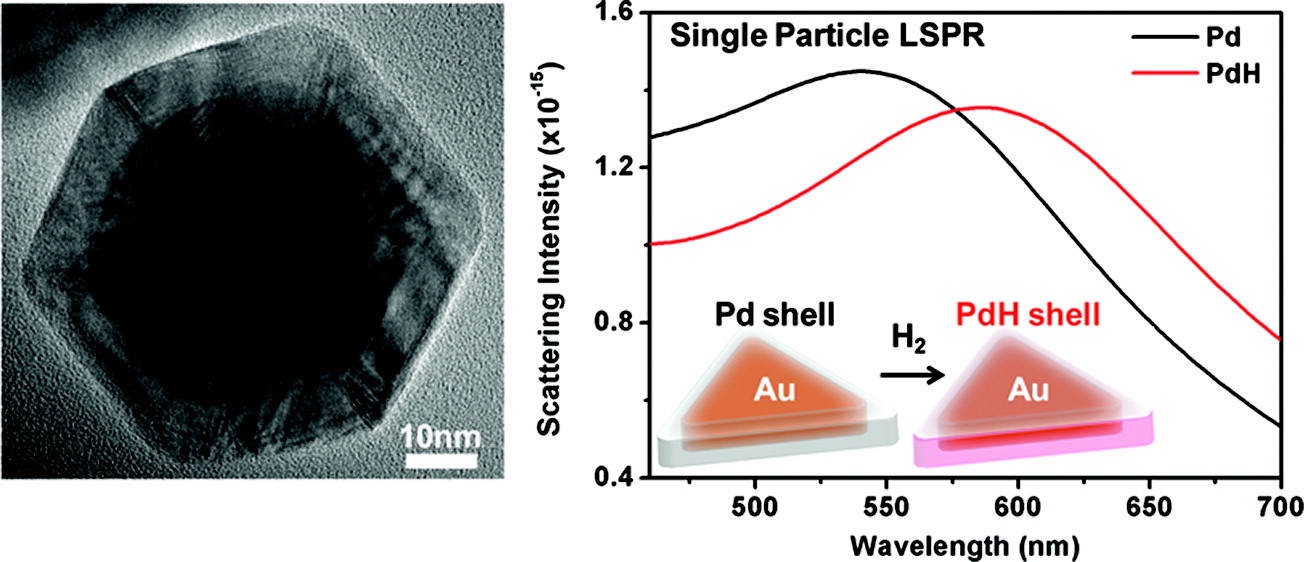
In this work, H2 absorption and desorption in faceted, crystalline Au/Pd core/shell nanocrystals and their interaction with a SiOx/Si support were studied at the single-particle level. Dark-field microscopy was used to monitor the changing optical properties of these Au/Pd nanoparticles (NPs) upon exposure to H2 as reversible H2 uptake from the Pd shell proceeded. Analysis of the heterogeneous ensemble of NPs revealed the H2 uptake trajectory of each nanocrystal to be shape-dependent. Differences in particle uptake trajectories were observed for individual particles with different shapes, faceting, and Pd shell thickness. In addition to palladium hydride formation, the single-particle trajectories were able to decipher specific instances where palladium silicide formation and Au/Pd interdiffusion occurred and helped us determine that this was more frequently seen in those particles within an ensemble having thicker Pd shells. This noninvasive, plasmonic-based direct sensing technique shows the importance of single-particle experiments in catalytically active systems and provides a foundation for studying more complex catalytic processes in inhomogeneous NP systems.
2005-2010....................................................................................................................................
Silicon-based photonic devices dissipate substantially less power and provide a significantly greater information bandwidth than electronic components. Unfortunately, large-scale integration of photonic devices has been limited by their large, wavelength-scale size and the weak optical response of Si. Surface plasmons may overcome these two limitations. Combining the high localization of electronic waves with the propagation properties of optical waves, plasmons can achieve extremely small mode wavelengths and large local electromagnetic field intensities. Si-based plasmonics has the potential to not only reduce the size of photonic components to deeply-subwavelength scales, but also to enhance the emission, detection, and manipulation of optical signals in Si. In this article, we discuss recent advances in Si-based plasmonics, including subwavelength interconnects, modulators, and emission sources. From scales spanning slab waveguides to single nanocrystals, we show that Si-based plasmonics can enable optical functionality competitive in size and speed with contemporary electronic components.
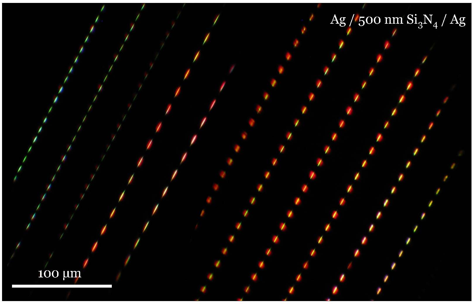
We report a method for filtering white light into individual colors using metal−insulator−metal resonators. The resonators are designed to support photonic modes at visible frequencies, and dispersion relations are developed for realistic experimental configurations. Experimental results indicate that passive Ag/Si3N4/Au resonators exhibit color filtering across the entire visible spectrum. Full field electromagnetic simulations were performed on active resonators for which the resonator length was varied from 1−3 μm and the output slit depth was systematically varied throughout the thickness of the dielectric layer. These resonators are shown to filter colors based on interference between the optical modes within the dielectric layer. By careful design of the output coupling, the resonator can selectively couple to intensity maxima of different photonic modes and, as a result, preferentially select any of the primary colors. We also illustrate how refractive index modulation in metal−insulator−metal resonators can yield actively tunable color filters. Simulations using lithium niobate as the dielectric layer and the top and bottom Ag layers as electrodes indicate that the output color can be tuned over the visible spectrum with an applied field.
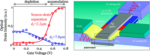
Realization of chip-based all-optical and optoelectronic computational networks will require ultracompact Si-compatible modulators, ideally comprising dimensions, materials, and functionality similar to electronic complementary metal−oxide−semiconductor (CMOS) components. Here we demonstrate such a modulator, based on field-effect modulation of plasmon waveguide modes in a MOS geometry. Near-infrared transmission between an optical source and drain is controlled by a gate voltage that drives the MOS into accumulation. Using the gate oxide as an optical channel, electro-optic modulation is achieved in device volumes of half of a cubic wavelength with femtojoule switching energies and the potential for gigahertz modulation frequencies.
We present a theoretical analysis of planar plasmonic waveguides that support propagation of positive and negative index modes. Particular attention is given to the modes sustained by metal-insulator-metal (MIM), insulator-metal-insulator (IMI), and insulator-insulator-metal (IIM) geometries at visible and near-infrared frequencies. We find that all three plasmonic structures are characterized by negative indices over a finite range of visible frequencies, with figures of merit approaching 20. Moreover, using finite-difference time-domain simulations, we demonstrate that visible-wavelength light propagating from free space into these waveguides can exhibit negative refraction. Refractive index and figure-of-merit calculations are presented for Ag/GaP and Ag/Si3N4 - based structures with waveguide core dimensions ranging from 5 to 50 nm and excitation wavelengths ranging from 350 nm to 850 nm. Our results provide the design criteria for realization of broadband, visible-frequency negative index materials and transformation-based optical elements for two-dimensional guided waves. These geometries can serve as basic elements of three-dimensional negative-index metamaterials.
A diffusion bonding method has been developed that enables layer transfer of single crystal lithium niobate thin films to silicon substrates. A silver film was deposited onto both the silicon and lithium niobate surfaces prior to bonding, and upon heating, a diffusion bond was formed. Transmission electron microscopy confirms the interface evolution via diffusion bonding which combines interfacial diffusion, power law creep, and growth of (111) silver grains to replace the as-bonded interface by a single polycrystalline silver film. The transferred film composition was the same as bulk lithium niobate.
A nanoscale gap between two metal surfaces can confine propagating surface plasmon polaritons (SPPs) to very small dimensions, but this geometry makes it inherently difficult to image SPP propagation at high resolution. We demonstrate the near-field probing of these SPPs, propagating within a 50 nm thick Si3N4 waveguide with Ag cladding layers for frequencies ranging from the blue to the near-infrared. Using near-field SPP interferometry, we determine the wave vector, showing that the wavelength is shortened to values as small as 156 nm for a free-space wavelength of 532 nm.
Nanofabricated photonic materials offer opportunities for crafting the propagation and dispersion of light in matter. We demonstrate an experimental realization of a two-dimensional negative-index material in the blue-green region of the visible spectrum, substantiated by direct geometric visualization of negative refraction. Negative indices were achieved with the use of an ultrathin Au-Si3N4-Ag waveguide sustaining a surface plasmon polariton mode with antiparallel group and phase velocities. All-angle negative refraction was observed at the interface between this bimetal waveguide and a conventional Ag-Si3N4-Ag slot waveguide. The results may enable the development of practical negative-index optical designs in the visible regime.
We report experimental realization of subwavelength slot waveguides that exhibit both micrometer-range propagation and high spatial confinement of light. Attention is given to rectangular waveguides with a Si3N4 core and Ag cladding; core thicknesses of 50−100 nm and widths of 250 nm − 10 μm are explored. Propagation lengths of 5λ are achieved with light confined to lateral and transverse dimensions of λ/5 and λ/2, respectively. This unique combination of light localization and propagation is achieved via interacting surface plasmons, which produce short modal wavelengths and strong field confinement at each metal/dielectric interface.
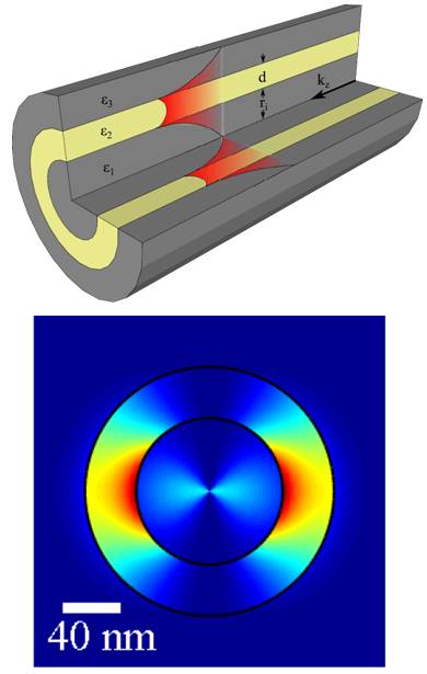
We present a numerical analysis of surface plasmon waveguides exhibiting both long-range propagation and spatial confinement of light with lateral dimensions of less than 10% of the free-space wavelength. Attention is given to characterizing the dispersion relations, wavelength-dependent propagation, and energy density decay in two-dimensional Ag∕SiO2∕Ag structures with waveguide thicknesses ranging from 12 nm to 250 nm. As in conventional planar insulator-metal-insulator (IMI) surface plasmon waveguides, analytic dispersion results indicate a splitting of plasmon modes—corresponding to symmetric and antisymmetric electric field distributions—as SiO2 core thickness is decreased below 100 nm. However, unlike IMI structures, surface plasmon momentum of the symmetric mode does not always exceed photon momentum, with thicker films (d∼50 nm) achieving effective indices as low as n=0.15. In addition, antisymmetric mode dispersion exhibits a cutoff for films thinner than d=20 nm, terminating at least 0.25 eV below resonance. From visible to near infrared wavelengths, plasmon propagation exceeds tens of microns with fields confined to within 20 nm of the structure. As the SiO2 core thickness is increased, propagation distances also increase with localization remaining constant. Conventional waveguiding modes of the structure are not observed until the core thickness approaches 100 nm. At such thicknesses, both transverse magnetic and transverse electric modes can be observed. Interestingly, for nonpropagating modes (i.e., modes where propagation does not exceed the micron scale), considerable field enhancement in the waveguide core is observed, rivaling the intensities reported in resonantly excited metallic nanoparticle waveguides.
A numerical analysis of surface plasmon dispersion, propagation, and localization on smooth lossy films is presented. Particular attention is given to determining wavelength-dependent behavior of thin Ag slab waveguides embedded in a symmetric SiO2 environment. Rather than considering Ag as a damped free electron gas, the metal is defined by the experimentally determined optical constants of Johnson and Christy and Palik. As in free electron gas models, analytic dispersion results indicate a splitting of plasmon modes—corresponding to symmetric and antisymmetric field distributions—as film thickness is decreased below 50 nm. However, unlike free electron gas models, the surface plasmon wave vector remains finite at resonance with the antisymmetric-field plasmon converging to a pure photon mode for very thin films. In addition, allowed excitation modes are found to exist between the bound and radiative branches of the dispersion curve. The propagation characteristics of all modes are determined, and for thin films (depending upon electric field symmetry), propagation distances range from microns to centimeters in the near infrared. Propagation distances are correlated with both the field decay (skin depth) and energy density distribution in the metal and surrounding dielectric. While the energy density of most long-range surface plasmons exhibits a broad spatial extent with limited confinement in the waveguide, it is found that high-field confinement does not necessarily limit propagation. In fact, enhanced propagation is observed for silver films at ultraviolet wavelengths despite strong field localization in the metal. The surface plasmon characteristics described in this paper provide a numerical springboard for engineering nanoscale metal plasmon waveguides, and the results may provide a new avenue for integrated optoelectronic applications.
Since the development of the light microscope in the 16th century, optical device sizeand performance have been limited by diffraction.Optoelectronic devices of today aremuch bigger than the smallest electronic devices for this reason.Achieving control oflight–material interactions for photonic device applications at the nanoscale requiresstructures that guide electromagnetic energy with subwavelength-scale modeconfinement.By converting the optical mode into nonradiating surface plasmons,electromagnetic energy can be guided in structures with lateral dimensions of less than10% of the free-space wavelength.A variety of methods—including electron-beamlithography and self-assembly—have been used to construct both particle and planarplasmon waveguides.Recent experimental studies have confirmed the strongly coupledcollective plasmonic modes of metallic nanostructures.In plasmon waveguidesconsisting of closely spaced silver rods, electromagnetic energy transport over distancesof 0.5m has been observed.Moreover, numerical simulations suggest the possibility ofmulti-centimeter plasmon propagation in thin metallic stripes.Thus, there appears to beno fundamental scaling limit to the size and density of photonic devices, and ongoingwork is aimed at identifying important device performance criteria in the subwavelengthsize regime.Ultimately, it may be possible to design an entire class of subwavelength-scale optoelectronic components (waveguides, sources, detectors, modulators) thatcould form the building blocks of an optical device technology—a technology scalable to molecular dimensions, with potential imaging, spectroscopy, and interconnectionapplications in computing, communications, and chemical/biological detection.
By the mid-17th century, numerous scientists—notably including Hooke and Gallileo—had developed transparent ground lenses and applied them in the construction of compound optical microscopes. This development revolutionized the contemporary understanding of the natural world by, for example, enabling the imaging of blood cells and microbes. Ever since this now bygone era of fantastic development of optics principles and instrumentation, the size and performance of photonic devices has been largely limited by diffraction. Photonic devices of today are generally composed of dielectric materials with modest dielectric constants, and are much bigger than the smallest electronic devices (e.g., transistors in silicon integrated circuits) for this reason.